IPP08CN10L G
OptiMOS®2 Power-Transistor
Product Summary
Features
V DS
• N-channel, logic level
R DS(on),max
8
m:
ID
98
A
• Excellent gate charge x R DS(on) product (FOM)
100
V
• Very low on-resistance R DS(on)
• 175 °C operating temperature
• Pb-free lead plating; RoHS compliant
• Qualified according to JEDEC1) for target application
• Ideal for high-frequency switching and synchronous rectification
Type
IPP08CN10L G
Package
PG-TO220-3
Marking
08CN10L
Maximum ratings, at T j=25 °C, unless otherwise specified
Parameter
Symbol Conditions
Continuous drain current
ID
Value
T C=25 °C
98
T C=100 °C
70
Pulsed drain current2)
I D,pulse
T C=25 °C
392
Avalanche energy, single pulse
E AS
I D=98 A, R GS=25 :
254
Reverse diode dv /dt
dv /dt
I D=95 A, V DS=80 V,
di /dt =100 A/μs,
T j,max=175 °C
6
Gate source voltage3)
V GS
Power dissipation
P tot
Operating and storage temperature
T j, T stg
T C=25 °C
IEC climatic category; DIN IEC 68-1
Rev. 0.6
Unit
A
mJ
kV/μs
±20
V
167
W
-55 ... 175
°C
55/175/56
page 1
2007-08-30
�IPP08CN10L G
Parameter
Values
Symbol Conditions
Unit
min.
typ.
max.
-
-
0.9
minimal footprint
-
-
62
6 cm2 cooling area 5)
-
-
40
100
-
-
Thermal characteristics
Thermal resistance, junction - case
Thermal resistance, junction
ambient
4)
-
R thJC
R thJA
K/W
Electrical characteristics, at T j=25 °C, unless otherwise specified
Static characteristics
Drain-source breakdown voltage
V (BR)DSS V GS=0 V, I D=1 mA
Gate threshold voltage
V GS(th)
V DS=V GS, I D=130 μA
1.2
1.85
2.4
Zero gate voltage drain current
I DSS
V DS=100 V, V GS=0 V,
T j=25 °C
-
0.1
1
V DS=100 V, V GS=0 V,
T j=125 °C
-
10
100
V
μA
Gate-source leakage current
I GSS
V GS=20 V, V DS=0 V
-
1
100
nA
Drain-source on-state resistance
R DS(on)
V GS=4.5 V, I D=49 A
-
7.7
10.4
m:
V GS=10 V, I D=98 A
-
6.6
8
-
1.3
-
:
83
166
-
S
Gate resistance
RG
Transconductance
g fs
1)
|V DS|>2|I D|R DS(on)max,
I D=98 A
J-STD20 and JESD22
2)
See figure 3
3)
Tjmax=150 °C and duty cycle D=0.01 for Vgs2|I D|R DS(on)max
g fs=f(I D); T j=25 °C
parameter: T j
200
220
200
180
150
160
g fs [S]
I D [A]
140
100
120
100
80
60
50
40
175 °C
20
25 °C
0
0
0
2
4
6
Rev. 0.6
0
40
80
120
160
I D [A]
V GS [V]
page 5
2007-08-30
�IPP08CN10L G
9 Drain-source on-state resistance
10 Typ. gate threshold voltage
R DS(on)=f(T j); I D=98 A; V GS=10 V
V GS(th)=f(T j); V GS=V DS
parameter: I D
20
2.5
2
1300 μA
130 μA
10
V GS(th) [V]
R DS(on) [m:]
15
98 %
1.5
1
typ
5
0.5
0
0
-60
-20
20
60
100
140
180
-60
-20
20
60
100
140
180
T j [°C]
T j [°C]
11 Typ. capacitances
12 Forward characteristics of reverse diode
C =f(V DS); V GS=0 V; f =1 MHz
I F=f(V SD)
parameter: T j
104
103
Ciss
Coss
25 °C
175 °C, 98%
102
25 °C, 98%
I F [A]
C [pF]
103
Crss
175 °C
102
101
101
100
0
20
40
60
80
V DS [V]
Rev. 0.6
0
0.5
1
1.5
2
V SD [V]
page 6
2007-08-30
�IPP08CN10L G
13 Avalanche characteristics
14 Typ. gate charge
I AS=f(t AV); R GS=25 :
V GS=f(Q gate); I D=98 A pulsed
parameter: T j(start)
parameter: V DD
1000
12
10
100
V GS [V]
I AS [A]
8
25 °C
100 °C
150 °C
10
80 V
50 V
6
20 V
4
2
1
0
1
10
100
1000
0
20
40
60
80
100
Q gate [nC]
t AV [μs]
15 Drain-source breakdown voltage
16 Gate charge waveforms
V BR(DSS)=f(T j); I D=1 mA
115
V GS
Qg
V BR(DSS) [V]
110
105
V g s(th)
100
95
Q g(th)
Q sw
Q gs
90
-60
-20
20
60
100
140
Q g ate
Q gd
180
T j [°C]
Rev. 0.6
page 7
2007-08-30
�IPP08CN10L G
PG-TO220-3: Outline
Rev. 0.6
page 8
2007-08-30
�IPP08CN10L G
Published by
Infineon Technologies AG
81726 Munich, Germany
© Infineon Technologies AG 2007.
All Rights Reserved.
Legal disclaimer
The information given in this data sheet shall in no event be regarded as a guarantee of conditions or
characteristics (“Beschaffenheitsgarantie”). With respect to any examples or hints given herein, any typical
values stated herein and/or any information regarding the application of the device, Infineon Technologies
hereby disclaims any and all warranties and liabilities of any kind, including without limitation warranties of
non-infringement of intellectual property rights of any third party.
Information
For further information on technology, delivery terms and conditions and prices please contact your nearest
Infineon Technologies Office (www.infineon.com ).
Warnings
Due to technical requirements components may contain dangerous substances. For information on the types
in question please contact your nearest Infineon Technologies Office.
Infineon Technologies Components may only be used in life-support devices or systems with the express
written approval of Infineon Technologies, if a failure of such components can reasonably be expected to
cause the failure of that life-support device or system, or to affect the safety or effectiveness of that device or
system. Life support devices or systems are intended to be implanted in the human body, or to support and/or
maintain and sustain and/or protect human life. If they fail, it is reasonable to assume that the health of the
user or other persons may be endangered.
Rev. 0.6
page 9
2007-08-30
�
很抱歉,暂时无法提供与“IPP08CN10L G”相匹配的价格&库存,您可以联系我们找货
免费人工找货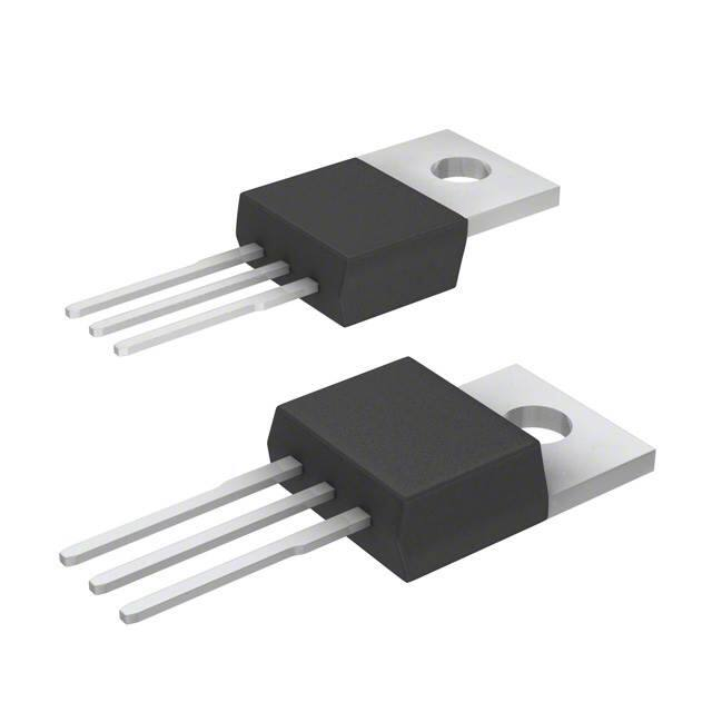


 工商网监
湘ICP备2023018690号
工商网监
湘ICP备2023018690号
